3-step HDI PCB | HYG603R12006A
Product Image
Product Details
Special Request:
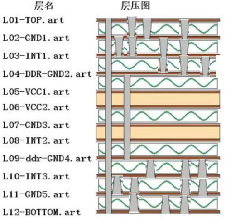
1. 3-step HDI PCB.
2. The blind vias are located between layers L1-12, L2-L3, L3-L4,
L9-L10, L10-L11, and L11-L12, as well as L9-L12. They are
laser-drilledand require copper filling and capping.
3. Impedance Control.
4. BGA Ball PAD: 0.3mm, BGA Elliptical PAD: 0.25mm.
Layer: 12L
Base Material: FR4 TG170℃
Board Thickness: 1.143mm
Outer Layer Final Copper Thickness: 1OZ
Inner Layer Final Copper Thickness: 0.5OZ&1OZ
Surface Finished: ENIG
Unit Size(mm): 91.60*201.40
Min. W/S(mil): 2.95/2.99
Min. Hole Size: 0.125mm
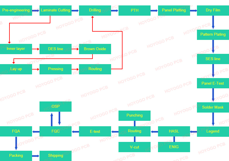
Production Process
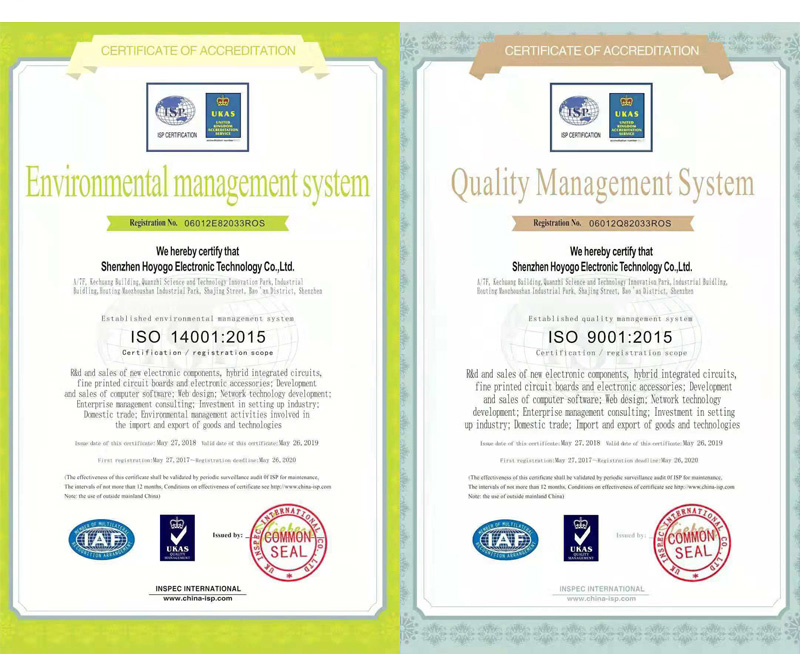
ISO Certification
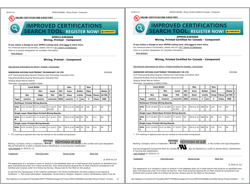
UL Certification
Application areas

Who will be our parters
FAQ
-
What’s your quality standard? What’s certificates do you have?
-
Our production is strictly following high quality system of automotive products, we certified with ISO9001, ISO14001, ISO13485 and IATF16949 and C-UL-S. All products strictly follow acceptance standard IPC-A-600-H and IPC-6012.
Contact us
Welcome to the HOYOGO website!
HONGKONG HOYOGO TECHNOLOGY CO.,LTD
SHENZHEN HOYOGO ELECTRONIC TECHNOLOGY CO.,LTD
Tel : (+86)-755-2300 1582
Fax : (+86)-755-2720 6126
Email : sales@hygpcb.com
Add: 7A Quanzhi Science and Technology Innovation Park,Shajing Street, Bao'an District, Shenzhen. 518104/ P.R.C.


 English
 Français
 Deutsch
 Português
 Pусский
 中文
中文