HYG089R04365A
Product Image
Product Details
Special Request:
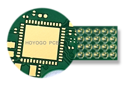
1. 1-step HDI Blind and Buried Via PCB.
2. Blind via holes made by laser need to be filled
with resin+ copper capped plating of filled via holes.
3. Impedance Control.
Layer: 4L
Base Material: FR4 IT150GTC, PP: IT-150GBS
Board Thickness: Non-antenna Area: 0.5+/-0.1mm;
Antenna Area: 0.428+/-0.1mm
Outer Layer Final Copper Thickness: 30um
Inner Layer Final Copper Thickness: 25um
Base Copper Thickness: 1/3OZ
Surface Finished: ENIG
Unit Size(mm): 28.63*30.40
Min. W/S(mil): 3.94/3.94
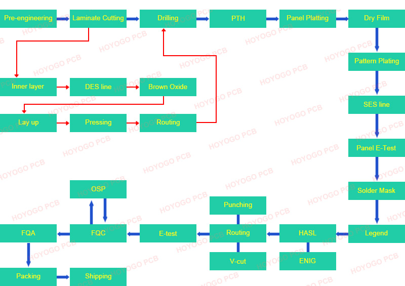
Min. Hole Size: 0.1mm Production Process
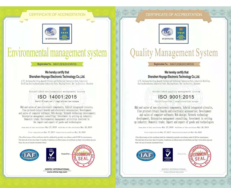
ISO Certification

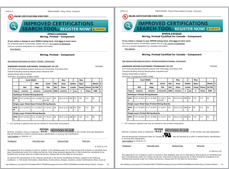
UL Certification

Application areas

Who will be our parters

FAQ
-
What kind of board can you offer? How about the layer count and base material?
-
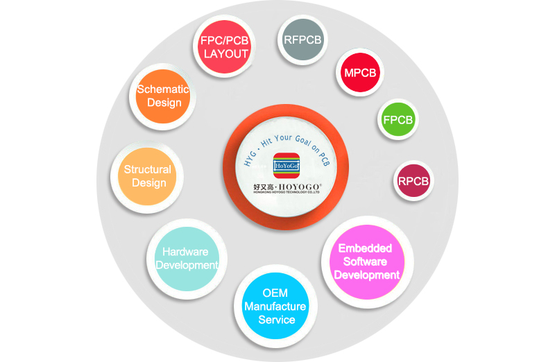
HoYoGo can offer board of HDI, gold finger, hard gold, flexible, rigid-flex, metal base, quick-turn around and PCBA. The layer is normally from 1 to 28layer. The base material also depends on the requirement, it can be KB or shengyi, etc.
Contact us
Welcome to the HOYOGO website!
HONGKONG HOYOGO TECHNOLOGY CO.,LTD
SHENZHEN HOYOGO ELECTRONIC TECHNOLOGY CO.,LTD
Tel : (+86)-755-2300 1582
Fax : (+86)-755-2720 6126
Email : sales@hygpcb.com
Add: 7A Quanzhi Science and Technology Innovation Park,Shajing Street, Bao'an District, Shenzhen. 518104/ P.R.C.

