[Product details]
|
|
|
|

|
|
Layer:4 |
Base Material:FR4 |
|
Board Thickness:1.6mm |
Unit Size:371 x 240 mm |
|
Min hole size:0.3mm |
Panel Size:371 x 250 mm |
|
Total Holes:1688 |
Copper OZ :2OZ |
|
Silkscreen:White |
Min Hole Copper Thickness:20um |
|
Surface Finishing:HASL Lead Free |
Solder Mask:Red |
[Feature]
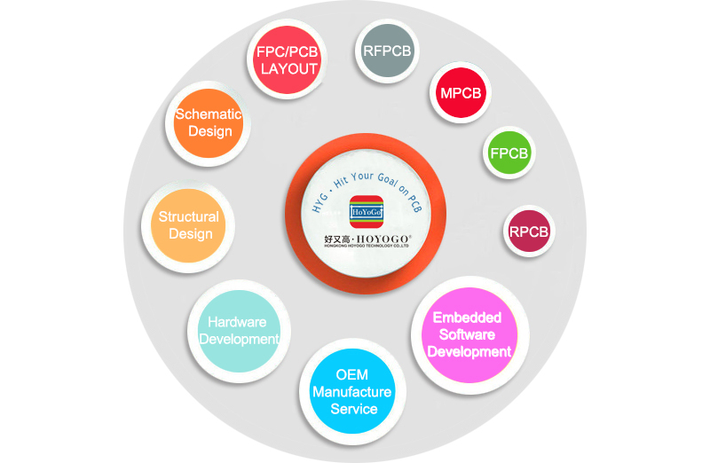
1, 1-16 layers of difficult production, HDl, buried / blind hole, high frequency board, high TG thick copper, aluminum plate, soft board and soft silver combined board and other circuit boards
2, single board, FR4 single-sided, double-sided, multi-layer board, single-sided double-sided aluminum, single-sided FPC, high-frequency board, etc.
3, Surface Finishing process: HASL Lead Free,HASL Lead,ENIG Thickness,Immersion Silver,OSP,Immersion Tin,Pressfit hole,Edge plating, Gold finger,Carbon Ink,Peelable mask,Punching,Depth milling etc.
4, proofing, copy board, large-scale production, multi-layer spray tin board proofing rush, mass production, 24 hours proofing, open mold timely.
[Proofing production time]
1, HASL Lead proofing: 1 day (fast 24 hours), multi-layer HASL Lead 2 days (fast 48 hours), 4/6 Layer HASL Lead: 3 days (expedited 72 hours) eight Layer HASL Lead: 4 days (expressed 96 hours)
2, small batch: 5-7 days, depending on the amount, multi-layer HASL Lead about 8 days
3, large quantities: 7-8 days, multi-layer HASL Lead 10-12 days
[Application]
HOYOGO Company's products are widely used in computer communications, home appliances, optoelectronics, positioning systems, medical equipment, video communications, instrumentation, automotive panels, etc.

|

|
[PCB ink FAQ]
1. Ink uneven
The surface ink cannot be evenly attached to the dots or the white dots of the ink (can't print)
Residues (pre-clean)
2. Large copper surface vacuoles
(1) Separation of ink and copper surfaces in full ink coverage on large copper surfaces
(2) Separation of ink and copper surfaces in the full coverage area of large copper or circuit surface corner inks
3. Plug holes
(1) Overflow of ink after exposure
(2) Overflow of ink after post baking
(3) ink overflow after spraying tin


Welcome to the HOYOGO website!
HONGKONG HOYOGO TECHNOLOGY CO.,LTD
SHENZHEN HOYOGO ELECTRONIC TECHNOLOGY CO.,LTD
Tel : (+86)-755-2300 1582
Fax : (+86)-755-2720 6126
Email : sales@hygpcb.com
Add: 7A Quanzhi Science and Technology Innovation Park,Shajing Street, Bao'an District, Shenzhen. 518104/ P.R.C.
