Welcome to visit Hoyogo website, let's connect the world together!
Customer service hotline:+86 13723413985 or 400 058 2288
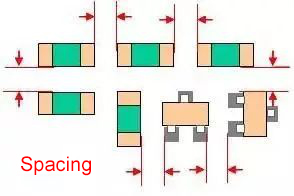
1. Spacing length between SMT
The spacing length between the components of the SMT is an issue that engineers must pay attention to when laying out. If the spacing length is too small, it is very difficult to print solder paste and avoid soldering.
The distance recommendations are as follows:
Device distance requirements between SMT:
Same Device: ≥0.3mm
Different Device: ≥0.13*h+0.3mm (h is the maximum height difference between neighboring components)
Distance requirments between parts that can only be assembled by hand: ≥1.5mm.
The above recommendations are for reference only, and can be based on the PCB process design specifications of the respective company.
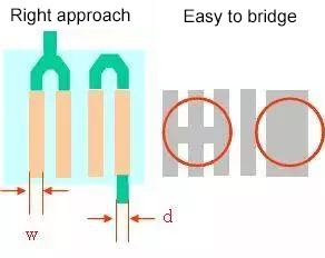
2. Distance between direct plug-in device and SMT.
As shown in the figure above, a sufficient distance should be maintained between direct plug-in device and SMT, and it is recommended to be between 1-3mm. Due to the troublesome processing, the situation of using plug-in cards is rare now.
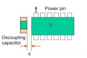
3. Placement of IC decoupling capacitors
Decoupling capacitors need to be placed near the power port of each IC as close as possible to the power port of the IC. When a chip has multiple power ports, a decoupling capacitor must be placed on each port.
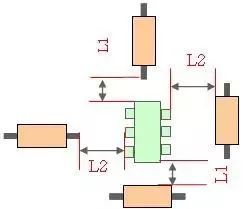
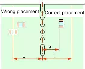
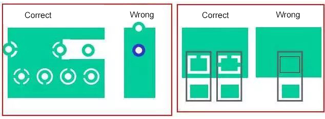
4. Please note the orientation and distance of components placed on the edge of the PCB
Since a panel PCB is generally used, the device needs to meet two condictions.
The first is parallel to the cutting direction. To make the mechanical stress of the device uniform. For example, if you place it as shown on the left of the figure above, when you split the panel, the stress directions of the two pads will be different, which may cause the the component and the pad to fall.
The second is that the devices cannot be arranged within a certain distance to prevent damage to the components when the board is cut.
5. Please note the need to be connect adjacent pads
If adjacent pads need to be connected, first make sure to connect them externally to prevent bridging. At this time, pay attention to the width of the copper wire.
6. If the pad falls in the common area, you need to consider the heat dissipation
If the pad falls in the area of the port, you should connect the pad to the port using the correct method on the right, and determine whether to connect 1 wire or 4 wires according to the current.
If the method shown in the left figure above is adopted, the temperature is completely spread due to the spread of copper, making welding or repairing and disassembling the components more difficult, so that welding cannot be performed.
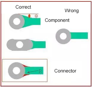
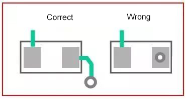
7. If the lead is smaller than the plug pad, you need to add a teardrop.
If the wire is smaller than the pad of the plug-in device, teardrops need to be added. As shown on the right of the figure above.
Adding teardrops has the following advantages:
1. Avoiding the sudden reduction in signal line width and causing reflections can make the connection between the traces and the component pads transition smoothly.
2. The problem that the connection between the pad and the trace is easily broken by the impact force is solved.
3. Placing a teardrop can also make the PCB look more beautiful.
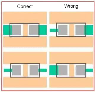
8. The width of the leads on both sides of the component pad must be the same.
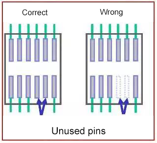
9. Please note that the pads of the unused pins are reserved and grounded
For example, in the picture above, two pins of a chip are not used, but the physical pins of the chip exist. If the two pins are left floating as shown on the right side of the figure above, it is easy to cause interference. If pads are added, they can be shielded to avoid interference.
10. It is best not to punch the via on the pads.
Please note that it is best not to punch vias on the pads, otherwise it will easily lead to tin lacking and false welding.
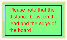
11. Please note the distance between the lead or component and the edge of the board
Please note that the leads or components cannot be too close to the edge of the board, especially single-sided boards. The general single-sided board is mostly a paper board, which is easy to break after being stressed. It will be affected if you wire or place components at the edges.
12. Neet to consider the ambient temperature of electrolytic capacitors away from heat sources.
At first, we need to consider whether the ambient temperature of the electrolytic capacitor meets the requirements. Second, the capacitor should be as far away from the heating area as possible to prevent the liquid electrolyte inside the electrolytic capacitor from drying out.


 English
 Français
 Deutsch
 Português
 Pусский
 中文
中文