Welcome to visit Hoyogo website, let's connect the world together!
Customer service hotline:+86 13723413985 or 400 058 2288
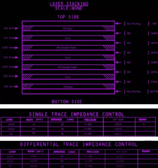
1. Signal lines that need impedance should be set strictly according to the line width and line spacing calculated by the stack. Such as RF signal (conventional 50R control), important single-ended 50R, differential 90R, differential 100R and other signal lines, the specific line width and spacing can be calculated by stacking.
2. The designed line width and line spacing should consider the production process capabilities of the selected PCB manufacturer. If the line width and line spacing set at the time of design exceeds the manufacturing capacity of the PCB manufacturer, the result is that unnecessary production costs will increase and may even lead to production failure. Under normal circumstances, the line width and line spacing are controlled to 6 / 6mil, and the through hole is 12mil (0.3mm). Basically, most PCB manufacturers can produce them, and the production cost is lower. The minimum line width and line spacing is controlled to 2 / 2mil, and the via hole is selected to be 4mil (0.1mm, at this time, it is generally a HDI blind buried via design, which requires laser vias). At this time, most PCB manufacturers can no longer produce, and the price is also the most expensive. The rule for setting the line width and line spacing here refers to the size between elements such as line-to-via, line-to-line, line-to-pad, line-to-via, and via-to-pad.
3. Setting rules requires consideration of design bottlenecks in the design file. For a 1mm BGA chip, the pin depth is shallow, and only one signal line is required between the two rows of pins, 6 / 6mil min. line width and line spacing can be set. If the pin depth is deep, two signal lines need to be run between the two rows of pins, then set to 4/4mil. For a 0.65mm BGA chip, usually set to 4/4 mil; for a 0.5mm BGA chip, the minimum line width and line spacing must be set to 3.5 / 3.5mil. For a 0.4mm BGA chip, HDI design is usually required. Generally, for design bottlenecks, regional rules can be set, local line widths and line spacings are set to small points, and line widths and line spacing in other locations in the PCB are set to be larger, in order to facilitate production and improve PCB qualification rates.
4. It needs to be set according to the density of the PCB design. The density is smaller, the circuit board will be looser, you can set the line width and line spacing to be a little larger, and vice versa. In general, you can follow these steps to set it up:
1) 8 / 8mil, the via is 12mil (0.3mm).
2) 6 / 6mil, the via is 12mil (0.3mm).
3) 4 / 4mil, the via is 8mil (0.2mm).
4) 3.5 / 3.5mil, the via is 8mil (0.2mm).
5) 3.5 / 3.5mil, via is 4mil (0.1mm, laser drilling).
6) 2 / 2mil, via hole is 4mil (0.1mm, laser drilling).


 English
 Français
 Deutsch
 Português
 Pусский
 中文
中文