|
Layer:4 |
Base Material:FR4+PI |
|
Board Thickness:1.82mm |
Unit size:300.37 x 80.16mm |
|
W/S(mil):4u |
Surface Finishing: ENIG Thickness |
|
Solder Mask:Green |
Copper OZ:1OZ |

|
Layer |
Quick service |
Standard service |
|
Double-sided |
3days |
10days |
|
4Layer |
5days |
12days |
|
6Layer |
6days |
14days |
|
8Layer |
7days |
15days |
|
10Layer |
8days |
18days |
|
10Layer above |
8-10days |
20days |

|

|

|

|

|

|

|
Item |
Flex pcb |
Rigid-Flex pcb |
|
Material |
PI,PET,PEN |
FR4+PI |
|
Layers |
1-12 |
2-12 |
|
Base copper thickness |
1/4-2OZ |
1/4-2OZ for flex,1/4-4oz for rigid |
|
Board dimension(Max) |
500mm x 800mm |
|
|
Via type |
Through hole, blind , buried |
|
|
Silkscreen Width/Space |
0.10mm |
|
|
Solder mask bridge |
0.20mm for coverlay ,0.12mm for LPI |
|
|
Drill |
0.15mm |
|
|
Punching |
0.5mm |
|
|
Ni/Auplating |
Ni:2-8um(80-320u”) Au:0.05-2um(2-80”) |
|
|
ENIG |
Ni:2-6um(80-240u”) Au:0.05-0.10um(2-4u”) |
|
|
Tin plating |
5-20um |
|
|
Immersion silver |
0.1-0.4um |
|
|
Immersion Tin |
0.5-1.5um |
|
|
OSP |
0.2um min |
|
|
Hard gold |
Hardness over 150HV |
|
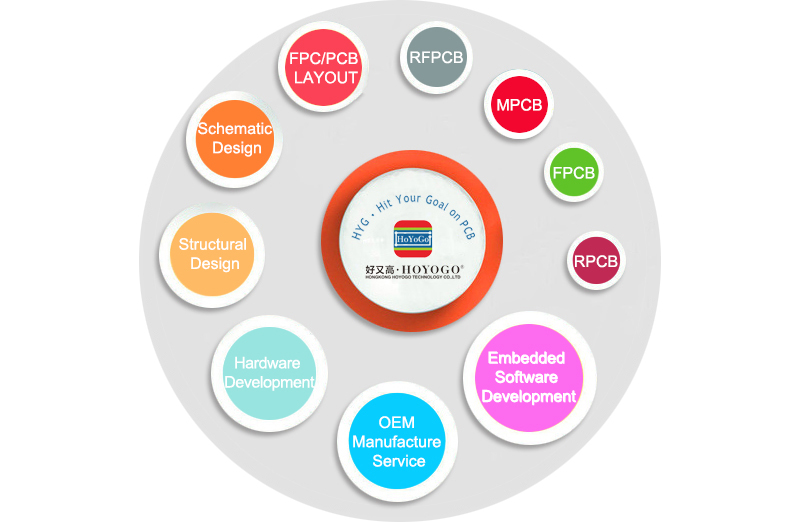
Special Techniques--Blind & Buried via, via in pad ,hard gold and gold fingers,Flash gold,Ni/Pd/Au finish,Edge plating.Depth control routing,Countersunk holes,etc
Special Services--FPC & Rigid/Flex quick turn, heavy copper mass production, IMS boards
PCBA Assembly Service--Small Volume and mass production

Characteristics of the flexible board: FPC is widely used in the occasions where dynamic structure is needed, and its bending resistance and pull resistance are its greatest characteristics!
Bend factors:
N1. Copper structure: The rolled copper has better tensile properties than ED copper. In the occasions where bending and pulling are required, it is generally necessary to use rolled copper!
N2. Minimum Tension Fatigue: In order to obtain the minimum tensile fatigue of the copper in the circuit, the press-fit structure of the FPC needs to be balanced!
N3. Bending radius: If the bending radius is large, the tension at the stress point can be reduced, and the bending life can be increased!
N4.FPC thickness: FPC thickness can reduce the stress of the copper wire

|

|
other factors:
1. Surface, smooth edge, pressure point
2. The stress point
3. The thickness of the glue, over-squeezing, and lack of glue all cause imbalance
4. Layering, poor structure may lead to rapid destruction of the line
5. Markable, PI edge is not smooth can cause tearing
6. Improper operation, copper wrinkles
7. improper STF structure, affect the bending area
8. Copper surface treatment will lead to structural imbalance

|
 |


Welcome to the HOYOGO website!
HONGKONG HOYOGO TECHNOLOGY CO.,LTD
SHENZHEN HOYOGO ELECTRONIC TECHNOLOGY CO.,LTD
Tel : (+86)-755-2300 1582
Fax : (+86)-755-2720 6126
Email : sales@hygpcb.com
Add: 7A Quanzhi Science and Technology Innovation Park,Shajing Street, Bao'an District, Shenzhen. 518104/ P.R.C.
